 Crystals 21.jpg)
| Code | Size | Thickness | Orientation | Surface Finish | Unit Price | Delivery | Cart |
|---|---|---|---|---|---|---|---|
| 641-001 | 5x5mm | 0.5mm | <100> | SSP | Inquire | 2 weeks | |
| 641-002 | 5x5mm | 0.5mm | <100> | DSP | Inquire | 2 weeks | |
| 641-003 | 5x5mm | 0.5mm | <110> | SSP | Inquire | 2 weeks | |
| 641-004 | 5x5mm | 0.5mm | <111> | SSP | Inquire | 2 weeks | |
| 641-005 | 10x10mm | 0.5mm | <100> | SSP | Inquire | 2 weeks | |
| 641-006 | 10x10mm | 0.5mm | <100> | DSP | Inquire | 2 weeks | |
| 641-007 | 10x10mm | 0.5mm | <110> | SSP | Inquire | 2 weeks | |
| 641-008 | 10x10mm | 0.5mm | <111> | SSP | Inquire | 2 weeks | |
| 641-009 | Φ12.7mm | 0.5mm | <100> | SSP | Inquire | 2 weeks | |
| 641-010 | Φ12.7mm | 0.5mm | <100> | DSP | Inquire | 2 weeks | |
| 641-011 | Φ25.4mm | 0.5mm | <100> | SSP | Inquire | 2 weeks | |
| 641-012 | Φ25.4mm | 0.5mm | <100> | DSP | Inquire | 2 weeks | |
| 641-013 | Φ50.8mm | 0.5mm | <100> | SSP | Inquire | 2 weeks | |
| 641-014 | Φ50.8mm | 0.5mm | <100> | DSP | Inquire | Inquire |
Due to its low dielectric constant and miniature loss at microwave band, and access to large-size MgO wafers, Single Crystal Magnesium Oxide (MgO) Wafers and Substrates have occupied substantial importance in the market of industrial HTS (High Temperature Superconductor) thin monocrystalline wafers for manufacturing high-temperature superconducting microwave filters and other devices required for mobile communication equipment. Other additional uses of MgO substrates include thin film growth of ferromagnetic, photoelectronic, and semiconductor. There is also an emerging interest in using MgO substrates for researching the epitaxial effects of substrates on the crystallization of polymers.
Hangzhou Shalom EO provides both stocked standard MgO wafers and custom MgO wafers.
Common Specifications:
| Material | MgO crystals | Orientation | <100>,<110>,<111> |
| Orientation Error | ±0.5° | Maximum Size | 50x50mm |
| Typical Thickness | 0.5mm, 1.0mm | Thickness Tolerance | ±0.05mm |
| Size Tolerance | ±0.1mm | Surface Finish | SSP or DSP |
| Roughness | Ra<0.5nm | Cleanness and Package | class 1000 clean room, class 100 bags |
MgO Properties:
| Growth Method | Special Arc Melting | Crystallographic Structure | Cubic a = 4.13 Å |
| Twinning Structure | Twin free | Orientation | <100>, <110>, <111> |
| Colour | Colourless | Transmission Range | 0.2 to 8 µm |
| Density | 3. 585 g/cm3 | Melting Point | 2780 +/- 20 °C |
| Thermal Expansion Coefficient | 11.2 * 10-6 K-1 | Dielectric Constant | 9.65 |
| Specific Resistivity | > 1017Ohm/cm |
Curves:
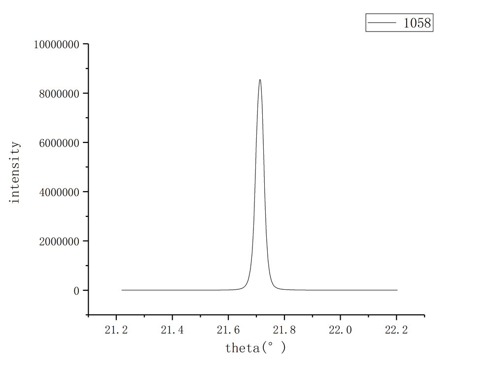
1)Typical X-Ray Diffraction (XRD) Curve of MgO <100> Crystals Substrates

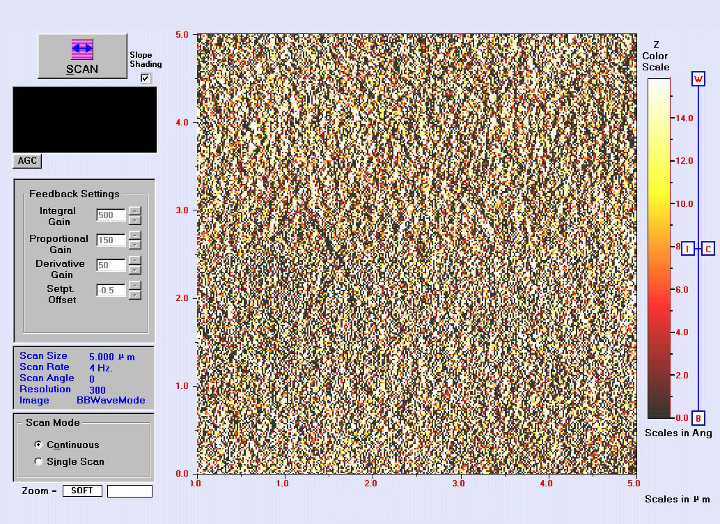
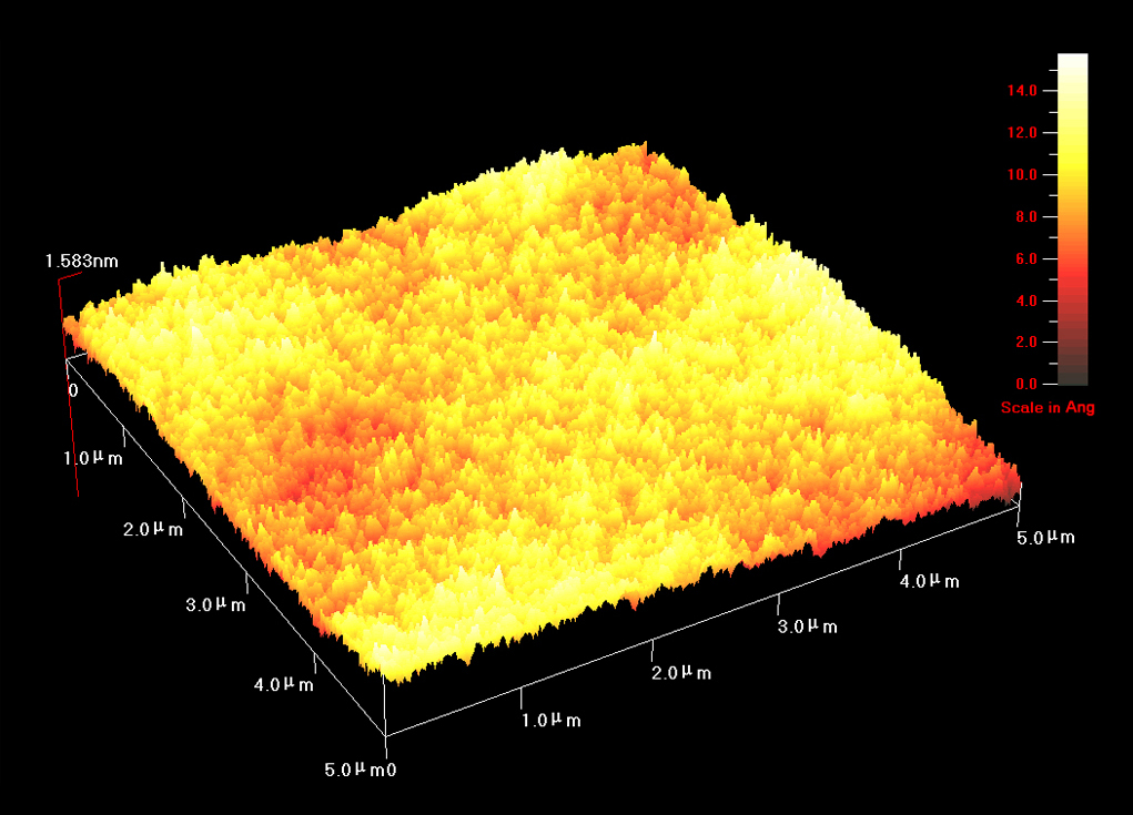
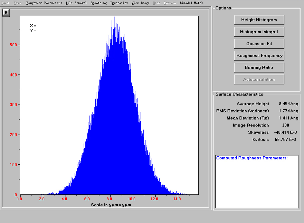
2) Typical Surface Roughness of MgO substrate <100> and <010> measured by Atomic Force Microscope (AFM) in 5μm x 5μm Scale


