
Sapphire (Aluminum Oxide, Al2O3) Substrate Properties
Overview:
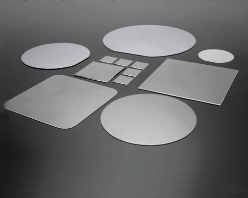
Aluminum oxide substrates are made of synthetic aluminum oxide crystals. Synthetic aluminum oxide crystals, with the chemical formula Al2O3, belong to the trigonal system and exhibit high hardness, excellent thermal stability, chemical inertness, and electrical insulation. They also possess a wide optical transmittance range and a low thermal expansion coefficient, making them suitable for applications in optics, electronics, microwaves, and wear-resistant coatings. The smooth, double-sided polished Al2O3 substrates are used in high-power electronic devices, insulating substrates, sensor windows, laser devices, and semiconductor epitaxial growth.
Artificial aluminum oxide crystals are typically produced by flame fusion, Czochralski, or heat exchange methods. The flame fusion method involves melting high-purity aluminum oxide powder at high temperatures in an oxyhydrogen flame. The molten droplets then crystallize layer by layer onto a seed crystal. By precisely controlling the powder supply and the seed crystal's descent rate, the crystal grows continuously along a defined orientation, ultimately forming an aluminum oxide ingot.
The Czochralski method melts high-purity aluminum oxide in a crucible. A seed crystal is slowly pulled upward from the melt surface while rotating, allowing the melt to cool and crystallize below the seed crystal, gradually forming a single crystal rod. This method can produce large, low-dislocation aluminum oxide crystals.
Physical and chemical properties of aluminum oxide crystals |
|
Crystal name |
Aluminum oxide crystals |
Crystal structure |
Hexagonal |
Lattice constant |
a = 4.748 A˚ c = 12.97 A˚ |
Melting point |
2040 ℃ |
density |
3.98 g/cm³ |
Mohs hardness |
9 mohs |
Refractive index (@600 nm) |
no=1.768, ne=1.760 @λ=546 nm |
Dielectric constant |
~9.4@300K A-axis; ~11.58@300K C-axis |
Thermal conductivity |
12 W/(m·K) |
Coefficient of thermal expansion |
7.5 × 10⁻⁶ /℃ |
Working principle:
Aluminum oxide (Al2O3) crystals possess a stable crystal structure and tunable lattice matching properties. When their lattice parameters closely match those of the functional thin film being deposited, the Al2O3 substrate can serve as an epitaxial substrate, guiding the orderly growth of thin film atoms along the substrate structure, resulting in a low-defect, high-performance single-crystal thin film. This lattice matching mechanism is the key foundation for achieving high-quality epitaxy.
Aluminum oxide exhibits excellent chemical and thermal stability, effectively preventing interfacial reactions and contamination, and safeguarding the intrinsic properties of thin film materials. Its high melting point and low thermal expansion coefficient enable the substrate to maintain structural integrity and dimensional stability during high-temperature deposition.
Aluminum oxide crystals have excellent optical transmittance and high dielectric strength, with good transmittance from the ultraviolet to the infrared region, making them suitable for optoelectronic devices and window components. By selecting substrates with different crystal orientations, the crystallization behavior and electrical properties of epitaxial films can be further controlled.
Production process
(1) Material preparation: This stage aims to prepare high-quality aluminum oxide crystal blanks. Common methods include the flame method, the Czochralski method, and the heat exchange method. The flame method process is as follows: high-purity aluminum oxide powder is fed into a hydrogen-oxygen flame to melt, and the molten droplets fall on the surface of the seed crystal. By controlling the temperature gradient and the descent rate, the melt is made to grow epitaxially along the seed crystal to form a single crystal. The Czochralski method process is as follows: high-purity aluminum oxide raw material is melted in an iridium crucible, the seed crystal contacts the molten liquid surface and is slowly pulled upward while rotating, so that the crystal continues to grow at the solid-liquid interface.
(2) Preliminary processing: After obtaining the crystal blank, quality inspection is first carried out, including defect detection and crystal orientation confirmation. Qualified blanks are directionally cut by high-precision cutting equipment to determine the crystal orientation of the substrate (such as c-plane, a-plane, r-plane, etc.) to meet different epitaxial requirements. After cutting, a substrate prototype of the predetermined shape and size is obtained.
(3) Precision machining: The substrate is milled and ground to remove the damage layer caused by cutting, and the thickness, parallelism, and flatness are controlled to strict tolerances. Mechanical polishing and chemical mechanical polishing (CMP) are then performed to gradually reduce the surface roughness, ultimately achieving nanometer-level or even sub-angstrom-level surface flatness.
(4) Cleaning and surface treatment: The polished substrate undergoes multiple ultrasonic and chemical cleaning to completely remove residues. If necessary, annealing treatment is performed to eliminate stress and stabilize the surface state.
Application areas:
Aluminum oxide substrates are widely used in high-power electronic devices, semiconductor epitaxial substrates, and optical windows due to their excellent insulation properties, high thermal conductivity, and good lattice matching. Aluminum oxide substrates can be used to grow third-generation semiconductor thin films such as gallium nitride (GaN), which are used to manufacture high-brightness LEDs, laser diodes, and radio frequency devices.
Aluminum oxide substrates can also be used as insulating substrates in the manufacture of microelectromechanical systems (MEMS), high-temperature sensors, and corrosion-resistant reaction chamber components. Their high surface hardness and chemical stability also make them ideal carriers for wear-resistant and biocompatible coatings. In the microwave field, aluminum oxide substrates are widely used in RF/microwave circuits, radar systems, and communications equipment, demonstrating low dielectric loss and high thermal conductivity.
Tags: synthetic sapphire crystal, al2o3 crystal, al2o3 crystal introduction